Tann Thona

Tann Thona

Telecommunication and Electronic Engineering

Post

Post Top Ad

Post Top Ad

Thursday, April 4, 2024

Smart Detecting Train Auto Control Gate

April 04, 2024 0

Royal University of Phnom Penh

Faculty of Engineering

Dep. of Telecommunication and Electronic Engineering


Course: Electronic System Design

Project Title:

Smart Detecting Train Auto Control Gate


Group member:

Ly Seyha, Tann Thona, Chhoy Noreath, Nop Da, Ham Sovann, Simpich Dany

Advisor: Chan Tola


1st Generation, Year 4th Semester I

2017-2018

Project Smart Detecting Train Auto Control Gate


Smart Detecting Train Auto Control Gate


I. Abstract

In this article, we aim to build an electronic project is a Smart Detecting Train Auto Control Gate to control traffic of the quadrilateral road of the train and cars road. In this project, we will use 3 main controllers; microcontroller, sensor, and servo motor. we have developed it by invented a new board as Arduino board by using an ATmega328P microcontroller instead of Uno Arduino to control the project process, IR sensor type of TCRT5000 to cooperate with our new board to detect the train coming and then feedback the signal to the microcontroller for control the traffic light, buzzer and servo motor for on/off gate to prevent accident of cars and the train. The invention of the new board is too many steps to do, we will show the board invention of each step in the detail of article below. We have made a new board in order to control the process instead of the Arduino board, so this is a powerful project that we can make a PCB by our own.

II. Introduction

In Cambodia, nowadays there is not so strong in using electronic system to control the system along the railroad, usually we see just the manual system in this case, so we will have an idea to make a system which it works automatically by electronic components in it. This is called Smart Detecting Train Auto Control Gate, it is an Arduino project which we built it with the process commonly as the reality in training process. It is working by automatically in detecting the coming train in a specific distance and then command to traffic light and on-off the gate. It is a powerful project that we have developed by using a main board of a new making PCB with a ATmega328 instead of using the Arduino board in controlling the whole process of our project. In this project, we have used two more important components: servo motors and sensors. we used IR sensor type TCRT5000 to detect train and feedback to a microcontroller while the train is coming for control the traffic light, buzzer and on/off gate to stop cars by servo motors for prevention accident at the quadrilateral road between cars road and railroad. There are 6 pairs of IR sensor along the two part of railroad which there are 3 pairs of sensors to control a direction and 3 more pairs to control another, we have arranged it because we have imagined that we need more safety and smoothly to process on it. Two servo motors are used in controlling in on/off gate when the train coming and across and the traffic light is just used LEDs to output.

We made it up in order to:
  • To learn about electronic components.
  • To show the powerful of electronic components in automatically working.
  • To understand the process in developing project and in reality
  • To compare process in project and reality working.
  • To know the designing of PCB by using software.
  • To know about making a new PCB as Arduino.
  • To show that we can making a controller PBC by our own selves.

III. Electronic Requirement

Base on this whole project, some requirement electronic components is list below:
  • Mini Servo x2
  • ATmega328P x1
  • Crystal 16MHz x1 and Capacitor Ceramic 22pF x2
  • IR sensor (TCRT5000) x6
  • LDR Sensor x1
  • LED (Red x3, Greenx2, Yellow x2 and White x8)
  • Resistor (10Kohm x7, 330ohm x 6 and 100ohm x2)
  • Capacitor Ceramic (100nF x2)
  • Capacitor Electrolyte 10uF x2
  • Adapter DC 9 or 12V (1 - 1.2A)
  • 12vDC Connector x1
  • Switch 12v x1
  • Terminal Block 2pins x1
  • Button x1
  • Regulator (L7805) x1
  • PCB (77mm x 72mm)
  • Jumper wire

1. TCRT5000 IR Sensor


There are two IR LEDs in a TCRT500 that blue LED is transmitter and black LED is a receiver. IR receiver is a potentiometer that is resistor has value depend on IR light.

It works by transmitter LEDs transmit the IR light while the receiver receives the IR light by reflecting signal from object to making change the resistance value. The resistance value of transmitter should be the same of LED’s resistance value and receiver should more than 1Kohm. See Figure 1 below for IR Sensor characteristic and Its working.


Figure 1: IR Sensor characteristic and Its working.


2. Servo Motor

In this project, we use servo motor to control to on-off gate when the train goes through that way.
  • It operates voltage from 4.8 – 6v
  • Stall torque: 1.8 kg.cm (4.8V), 2.2 kg.cm (6 V)
  • Operating speed: 0.1 s/60 degree (4.8 V), 0.08 s/60 degree (6 V).
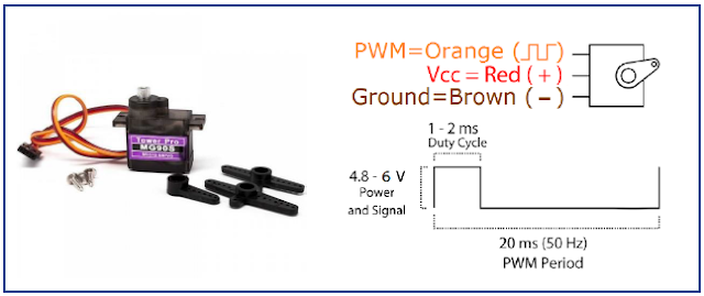
Figure 2: Servo motor specification.


3. ATmega328P

We used ATmega328P instead of Arduino board process of controlling, it is operating well with 1.8-5.5V of input voltage. It needed a crystal clock with two ceramic capacitors and a 10KOmh resistor and a button for reset to working our microcontroller.
  • Pin 1 is a reset pin to connect with a button.
  • Pins 2&3 are the Rx and Tx pins.
  • Pins 4 to 6 and 11 to 19 are the output digital pins.
  • For pins 7&8 are the power pins of VCC and GND.
  • For pins 9&10 are the connection pins of crystal with 2 capacitors.
  • For pins 23-28 are the output analog pins.

Figure 3: Pins connection diagram for ATmega328P.


IV. Methodology

1. Making Print Circuit Board(PCB)

1.1 PCB Software Design

Base on this project, we have used 2 kind of software programs of Proteus to make new a PCB:


Figure 4: Interface of Proteus ISIS design circuit schematic with v7.10.

Figure 5: Interface of Proteus ARES design layout diagram with v7.10.

  • Proteus ISIS software v7.10: is used to draw the circuit diagram by connecting from any components which we necessary need for our project. It is also corporates to an ARES software program. See Figure 4 below for ISIS design.
  • Proteus ARES software v7.10: used to draw a layout of PCB diagram which connect form ISIS schematic design. See Figure 5 below for ARES design layout diagram.
*Note: in these combining program, some package may not have in this software, so you need to draw it by manually.
Go to this link to download software of the Proteus.v7.10 for the designing circuit schematic and diagram: Download Proteus.v7.10 Software

1.2 PCB Hardware

After we already design the diagram in Proteus software, then we need to follow these below steps:


Figure 6: Making PCB hardware with step by step.


These above figures show the steps of how to make a new PCB:
  • For Fig6.1, show the printing out of the circuit drawing on a slipper paper by the Laserjet printer.
  • Fig6.2, Iron that printed paper on the PCB board with a specific size.
  • Fig6.3, Put the PCB which already ironed into acid and making vibrate it carefully.
  • After we finish these 3 steps above then we need to apply all components to PCB board of each its position and then soldering it one by one. See Fig6.4&6.5.

V. Experiment

1. Program on ATMEGA328P Microcontroller


This is the explains how to migrate from an Arduino board to a standalone the ATmega328P microcontroller on a breadboard for burning the bootloader and uploading program to it.

Unless you choose to use the minimal configuration described at the end of this tutorial, we'll need four main components (besides the Arduino, ATmega328, and breadboard):
  • a 16 MHz crystal,
  • a 10k resistor, and
  • two 18 or 22 picofarad (ceramic) capacitors.

1.1 Burning the Bootloader

We need to burn the bootloader onto a new ATmega328P microcontroller by using an Arduino board as an in-system program (ISP).


Figure 7: Wire connection to burn the bootloader onto an ATmega328P with Uno Arduino.


We’re choosing an Uno Arduino board for this section, so to burn the bootloader, we need to follow these below steps:
  • Firstly, need to upload the ArduinoISP sketch onto an original Arduino board by select the board and serial port from the Tools menu that correspond to our board.
  • Wire up the Arduino board and microcontroller as shown in the diagram of Figure7.
  • Select "Arduino Duemilanove" from the Tools -> Board menu and then select to ATmega328.
  • Select "Arduino as ISP" from Tools -> Programmer
  • Run Tools -> Burn Bootloader
You should only need to burn the bootloader once. After you've done so, you can remove the jumper wires connected to pins 10, 11, 12, and 13 of the Arduino board.

1.2 Uploading Using an Arduino Board

After ATmega328P has the Arduino bootloader on it, then we can upload programs to it by using the USB-to-serial convertor (FTDI chip) on an Arduino board.

  • To upload our code onto it, need to remove the microcontroller from the Uno Arduino board so the FTDI chip can talk to the microcontroller on the breadboard instead.
  • Connect the RX and TX lines from the Arduino board to our ATmega328 on the breadboard as shown in Figure 8.
  • To program the microcontroller, select "Arduino Duemilanove " from the the Tools > Board menu and select ATmega328, then upload as usual.

Figure 8: Wire connection to uploading sketches code to an ATmega328P on a breadboard.


1.3 Algorithm of Project

In this section, we will introduce you to know about our project processing in the diagram, see Figure 9 below to understand well.

To make a process in this project, we need to do the coding. For coding, you can download in link:


Figure 9: Processing of Smart Detecting Train Auto Control Gate.


Figure 10: Flow Char


VI. Result

After we spent 10 weeks to develop it, finally we have completed it with 90% of fully project.
According to this project, there are two main parts, the smart detecting train system and auto night light system on this project. Let see the result of our full project’s demo is in the link below.


Figure 11: Result of Smart Detecting Train Auto Control Gate.


VI. Conclusion

In sum, we have developed an electronic project which work automatically to traffic light and gate control by detecting the coming train at quadrilateral road. We have made a new PCB board which include a new chip ATmega328P and all-important components on it to cover to a whole project’s process that can be replacement to an Uno Arduino board. Finally, it is working 90% of fully project and we need to update it with any remaining part and something lost in order to finish our project completely.

After we have finished this project, we knew many things about this project:
  • Knew some electronic components characteristic and its specification.
  • Understood the process in developing project and in reality.
  • Know the comparing of process in project and reality working.
  • Understood well about the designing of PCB by using Proteus software.
  • Knew about how making a new PCB and boot-loading the ATmega328P as Arduino.


Reference


[1]. https://www.arduino.cc/en/Tutorial/ArduinoToBreadboard

[2]. https://nomada-e.com/store/sensores/9-sensor-optico-reflectivo-tcrt5000.html

[3]. http://full-parts.com/mg90s-metal-gear-servo-for-arduino-micro-tower-pro-180-degrees.html

[4]. https://voidyourwarranty.wordpress.com/2014/08/17/using-arduino-as-an-isp-to-program-a-standalone-atmega-328p-including-fuses/


Photos

Date: 20 December 2017
Location: Royal University of Phnom Penh, Cambodia


Read More

Stereo Audio Amplifier Using KA2209 (IC)

April 04, 2024 0

Royal University of Phnom Penh

Faculty of Engineering

Dep. of Telecommunication and Electronic Engineering


Project Title: Stereo Audio Amplifier


Group member:

Ly Seyha, Tann Thona, Chhoy Noreath, Nop Da, Simpich Dany

Advisor: Dr. Thap Tharoeun

First Generation, Year 3rd Semester II
2017


I. Introduction

This is a stereo audio amplifier module using the KA2209 IC, which is equivalent to the TDA2822. It will operate well from 3 – 12v DC and will work from a battery since the quiescent current drain is low. It requires no heat sink for normal use. The input and output are both ground referenced. Maximum output will be obtained with a 12v power supply and 8-ohm speaker, however it is particularly suitable for driving headphones from a supply as low as 3V.


II. Specifications of KA2209

  • D.C. input: 5 – 12 V at 200 – 500 mA max.
  • Power output: - > 1-Watt max. 4-8 ohms, 12V DC
  • > 500 mW, 32-ohm, 12V
  • > 500 mW, 4-ohm, 6V
  • Freq. Resp.: ~ 40 Hz to 200 kHz, 8-ohm, G=10
  • < 20 Hz to > 50 kHz, 32 ohms
  • THD: < 1 % @ 750 mW, 4-8Ω, 12V
  • < 0.2 % @ 250 mW, 4-8Ω, 12V
  • Sensitivity: < 300 mV, G = 20 dB
Figure 1. KA2209 IC


III. Assembly Instructions

  • The electrolytic capacitors are polarized, they have a + or - marked on them and they must be inserted correctly into the PCB.
  • The IC and socket have a notch at one end, which is marked on the PC board overlay. If there is no notch on the IC, there will be a dot next to pin 1, which is the same end.
  • Solder the socket in place first before installing the IC itself, then resistors, capacitors, and PCB pins. Leave the potentiometer until last. We have also provided input attenuation via the potentiometer which can be used as a volume control. This will keep the signal to noise ratio as high as possible. Extra gain provided by the amplifier will reduce the S/N ratio by a similar amount, since the input noise figure is constant.

IV. Testing

Check the voltage and polarity before connecting the battery or power supply. If it does not work, recheck all component positions and polarity. Check all solder joints, and all external wiring. The IC itself is quite robust, and there is very little else to go wrong. Remember when testing, it will not produce full output for more than a short duration because of limited heat dissipation. We found it easily exceeded the manufacturers specifications however.

IV. Circuit Description

There are only a few external components, 

  • R1, R2 and R3, R4 are the feedback resistors. 
  • C1 provides power supply decoupling.
  • C2, C3 are the output coupling capacitors.
  • C4, R1 and C5, R2 block DC in the feedback circuit from the inverting inputs.
  • C6, R3 and C7, R4 act as Zobel networks providing a high frequency load to maintain stability at frequencies where loud speaker inductive reactance may become excessive.
  • C8 and C9 are the input coupling capacitors, which block any DC that might be present on the inputs.
  • The pot provides adjustable input level attenuation.

Figure 2. Stereo Audio Circuit with KA2209 IC

V. Components Requirement

  • KA2209 IC   (x1)
  • Printed Circuit Board   (x1)
  • Capacitors
    • C1: 10 uF / 16 or 25V elec_cap   (x1)
    • C2, C3, C4, C5: 100 uF / 16 or 25V elec_cap   (x4)
    • C6, C7: 104 / 16V cera_cap   (x2)
    • C8, C9: 103 / cera_cap   (x2)
  • Resistor 4.7KOhm
    • R1, R2:  4.7 KOhm   (x2)
    • R3, R4:  3.3 KOhm   (x2)
  • Potentiometer: 10KOhm   (x1)

VI. Reference

Quasar Electronics Limited
PO Box 6935
Bishops Stortford
CM23 4WP
UNITED KINGDOM 
Website:    http://www.quasarelectronics.com/3087.htm


Photos


Date: 26 October 2017
Location: Royal University of Phnom Penh


Read More

Mobile Phone Broadcasting 1G, 2G, 3G, and 4G Field Strength Analysis

April 04, 2024 0

Mobile Phone Broadcasting (1G, 2G, 3G, and 4G) Field Strength Analysis in Royal University of Phnom Penh Zone

Ly Seyha, Cheasim Samnang, Pov Vannak, Ven Seyha, Tann Thona, Phan Theara, Chim Socheat, Nop Da, Keng Chhit, Long Ty, Ham Sovann, Chhory Noreath

Dept. of Telecommunication and Electronic Engineering, Royal University of Phnom Penh, Russia Federation Blvd (110), Cambodia 
{seyhaly.fe, samnangc96, vanakpov2, venseyha88, tannthona, theara.phan010, chimsocheat978, nopda.fe, kengchhit, longty096, hamsovann96, noreath.chhoy123}@gmail.com
All authors contributed equally to this work 

Abstract 

In this article is discussed about mobile phone field testing in Royal University of Phnom Penh (RUPP) zone by using Waveguide Horn antenna of maximum operated frequency 18GHz to received signal from the free-space. We used the high operate frequency spectrum analyzer (up to 9KHz – 22GHz) for scanning and analyses the signal from the Horn antenna of mobile phone of 1G (800-900MHz), 2G (900MHz-1.2GHz), 3G (1.2-1.8GHz), and 4G (1.8-2.1GHz). To analyses signal, we spent a day (9 hours) to test with 5 main locations in RUPP. After finish the experiment, we have got some information result and data statistic to analyses the comparison of power gain in the testing location and then make a conclusion for those data.

Keywords— Gain, Horn Antenna, Spectrum Analyzer, Power Testing, RF Environment Testing, Antenna Testing, Mobile Phone (1G, 2G, 3G, 4G) Testing Field.

I. INTRODUCTION 

 Nowadays, companies are using their own policies to broadcast frequency with the only power of 10KW to cover around Phnom Penh, but some companies did fail by broadcasting frequency with more than 10KW, Electromagnetic field is very effective to people health if the broadcasting of the strong power. Anyway, we have analyzed field effect in Royal University of Phnom Penh (RUPP) zone to understanding over power effective to people with RF Environment Analysis by using Horn Antenna and Spectrum Analyzer. At that time, we have spent a day (9 hours) to tested with 5 locations around Royal University of Phnom Penh (RUPP) with the different antenna height.
The information of locations of our experiment was held on the description below:

A. Location 1

The 1st location of our experiment was on the roof of building C in RUPP which represent the antenna height of 14m.
  • Address of Location: 11°34'12.9"N 104°53'27.1"E

B. Location 2

The 2nd location of our experiment was on the 4th floor of building B in RUPP which represent the antenna height of 15m.
  • Address of Location: 11°34'12.1"N 104°53'22.7"E

C. Location 3 

The 3rd location of our experiment was on the 6th floor of building A in RUPP which represent the antenna height of 25m.
  • Address of Location: 11°34'07.1"N 104°53'27.4"E

D. Location 4

The 4th location of our experiment was in front of CJCC building in RUPP zone which represent the antenna height of 1.2m.
  • Address of Location: 11°34'07.4"N 104°53'36.9"E

E. Location 5

The 5th location of our experiment was on the roof of CKCC building in RUPP which represent the antenna height of 13m.
  • Address of Location: 11°34'08.3"N 104°53'18.1"E


II. EQUIPMENT AND METHODS

To process this experiment of mobile phone testing field with generation type (1G, 2G, 3G, and 4G) we need some equipment such as:
  • Waveguide Horn Antenna (Model: hp 3115, Serial/No. 9901A5662): are very popular use at UHF (1 - 18GHz) and higher frequencies. Horn antennas often have a directional radiation pattern with a high antenna gain, which can range up to 25 dB in some cases, with 10 - 20 dB being typical. Horn antenna have very little loss, so the directivity of a horn is roughly equal to its gain. The radiation pattern of a horn antenna will depend on B and A (the dimensions of the horn at the opening) and R (the length of the horn, which also affects the flare angles of the horn), along with band a (the dimensions of the waveguide). These parameters are optimized in order to tailor the performance of the horn antenna, and are illustrated in the following Fig. 1.
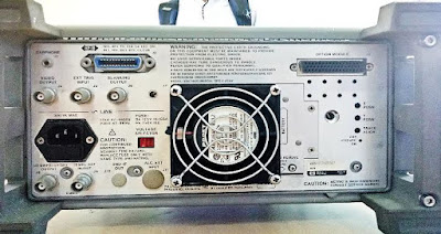
  • Spectrum Analyzer (Model: hp 8562A, Serial/No. 3017A05067): use it to measures the magnitude of an input signal versus frequency within the full frequency range of the instrument. The input signal that a spectrum analyzer measures is electrical. It operates well with input connector of 50ohm and frequency from 9KHz to 22GHz (see Fig. 2 for front panel), and the LINE input operates at normally 115V (47 – 440Hz) or at normally 230V (47 – 66Hz). See the back panel in the Fig. 3.
  • Compass: is also use in this experiment, it uses for finding the direction of the high-power performance from broadcasting power source.
  • GPS: use it to find the location of performance experiment.
Fig. 1 Geometry of the double ridged horn antenna.


Fig. 2 Spectrum analyzer model hp 8562A as front view.


Fig. 3 Spectrum analyzer model hp 8562A as back view.


III. EXPERIMENT

To process this fully experiment propose we did the test on the high position and testing it step by step. Firstly, we need to find a high position with no obstacle around, then let checking the environment around that location is it effective more or less, so try to find the better one of effective. After that we can start the experiment by:
  • Firstly, checking the AC input power that provide to Spectrum Analyzer, if AC power source fit to the Spectrum Analyzer input LINE containing, so the operate will starting.
  • Setting start and stop frequency of range from 700MHz to 2.9GHz to analyze the magnitude spectrum and frequency of mobile phone (1G, 2G, 3G, and 4G) by pushing on FREQUENCY button panel.
  • Start checking and cleaning the connector N-male type to protect the problem of Spectrum Analyzer because it works with the high frequency, then connect the Horn Antenna to Spectrum Analyzer via RF coaxial cable and N-male connector type of 50ohm impedance.
  • Press on TRACE button panel to do the MAX HOLD to signal, and then pushing VIEW to freeze the signal.
  • Let press on MARKER panel to check each magnitude spectrum power and frequencies that showing on Spectrum Analyzer’s monitor.
Checking it one by one until you finish your experiment propose of mobile phone testing with 1G, 2G, 3G, and 4G.
Environment is the main part of effective to analyze the data signal, it is also focus with the weather, so after you finish your signal testing, you need to checking about environment and weather in the detail.

IV. RESULTS AND DISCUSSIONS

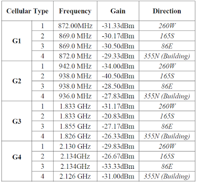
After we finished those experiment we have got some information about it and collected it in the table below.

  • TABLE I
RESULT OF EXPERIMENT OF LOCATION1 ON ROOF OF BUILDING C.


Fig. 4 Data of Location1.
  • TABLE II
RESULT OF EXPERIMENT OF LOCATION2 OF 4TH FLOOR, BUILDING B.

Fig. 5 Data of Location2.

  • TABLE III
RESULT OF EXPERIMENT OF LOCATION3 OF 6TH FLOOR, BUILDING A.

Fig. 6 Data of Location3.

  • TABLE IV
RESULT OF EXPERIMENT OF LOCATION4 IN FRONT OF CJCC BUILDING.

Fig. 7 Data of Location4.


  • TABLE V
RESULT OF EXPERIMENT OF LOCATION5 ON ROOF OF CKCC BUILDING.

Fig. 8 Data of Location5

According to TABLE I and Fig. 4, we can observe that:
  • For 1G, the direction East has the highest power gain among the three others (-27.5dBm) because there is no effective by any environment and maybe power source of 1G comes from this direction and the direction West has the lowest gain (-37.67dBm) because it has reflected by wall of building C.
  • For 2G, the direction South has the highest gain (-19.33dBm) among the three others because maybe the power source of 2G comes from this direction and the direction East has the lowest gain (-24.5dBw) because maybe the power source does not come from this direction.
  • For 3G, the direction North has the highest gain (-15.67dBm) among the three others because there is no effective by any environment and maybe power source of 3G comes from this direction and direction West has the lowest gain (-23.67dBw) because it is being reflected my wall of building C.
  • For 4G, the direction N has the highest gain (-18.83dBm) among the three others because there is no effective by any environment and maybe power source of 4G comes from this direction and the direction South has the lowest gain (-28.83dBw).
Base on TABLE II and Fig. 5, we can observe that:
  • For 1G, the direction North has the highest gain (-23.00dBm) among the three others because there is no effective by any environment and maybe power source of 1G comes from this direction and direction East has the lowest gain (-29.00dBw).
  • For 2G, the direction West has the highest power gain (-26.00dBm) among the three others and direction East has the lowest gain (-30.00dBw).
  • For 3G, the direction West has the highest power gain (-20.83dBm) among the three others and direction North has the lowest gain (-32.33dBw).
  • For 4G, the direction East has the highest power gain (-22.83dBm) among the three others and direction North has the lowest gain (-33.33dBw).
Base on TABLE III and Fig. 6, we can observe that:
  • For 1G, the direction North has the highest gain (-15.67dBm) among the three others and direction West has the lowest gain (-23.67dBw).
  • For 2G, the direction West has the highest gain (-24.83dBm) among the three others and direction South has the lowest gain (-32.83dBw).
  • For 3G, the direction West has the highest gain (-21.33dBm) among the three others and direction South has the lowest gain (-35dBw).
  • For 4G, the direction East has the highest gain (-20.83dBm) among the three others and direction South has the lowest gain (-42.17dBw).
According to TABLE IV and Fig. 7, we can observe that:
  • For 1G, the direction North has the highest gain (-29.33dBm) among the three others and direction East has the lowest gain (-30.5dBw).
  • For 2G, the direction North has the highest gain (-27.83dBm) among the three others and direction South has the lowest gain (-40.5dBw).
  • For 3G, the direction South has the highest gain (-20.83dBm) among the three others and direction West has the lowest gain (-31.17dBw).
  • For 4G, the direction South has the highest gain (-26.67dBm) among the three others and direction East has the lowest gain (-33.33dBw).
According to TABLE IV and Fig. 8, we can observe that:
  • For 1G, the direction North has the highest gain (-17.67dBm) among the three others and direction East has the lowest gain (-30dBw).
  • For 2G, the direction West has the highest gain (-24.33dBm) among the three others and direction South has the lowest gain (-34.17dBw).
  • For 3G, the direction East has the highest gain (-20.33dBm) among the three others and direction West has the lowest gain (-31.83dBw).
  • For 4G, the direction East has the highest gain (-26.33dBm) among the three others and direction South has the lowest gain (-32dBw).
In sum, the power Gain of those 5 locations can conclude that:
  • At the building C with 14m of height antenna is the best location has good power Gain because of the location of experiment is on the roof and maybe cause of no effective by environment (tree, high building...) and there is many station or repeater around this location.
  • At the location4 of in front of CJCC with the antenna height 1.2m where the location of ground which has a lot of obstacle of building and some trees effective around it and has the lowest gain if compared to others location of experiment.
  • For direction have reflection is OK that has the medium gain no problem.
For the generation type of mobile phone in Cambodia, we can conclude that:
  • For 1G, assume that it is the 1st generation that popularity in using of voice calling, so the broadcasting power also around.
  • For 2G, it is the 2nd generation technology that if compare to 1G, it uses to extent the number of users in a radio channel as digital, assume that it uses for voice and data signal as 1G, but it is not popular to use, so the signal is less.
  • For 3G, it is next generation of 2G, it uses for voice, data, and especially uses for video telephony and internet surfing. It is a high-speed network that also popularity in using, so that it is wide-band of broadcasting the gain power around the experiment.
  • For 4G is a recently generation which did not cover openly in Cambodia and it also include with the block of number of user, so the broadcasting power is less.


V. CONCLUSION

Totally, the experiment propose is to analyzes RF signal of mobile phone with 1G, 2G, 3G, and 4G, which broadcasting power from mobile phone station or its repeater by using a high frequency Spectrum Analyzer and Waveguide Horn Antenna.

After we got the data information from this experiment, according to these data will use to analyze which location has obstacle effective, reflected by the building, or any effective else, so that the result of Gain power that we got does depend on that effective environment.

A. In Case of High Gain Power

Usually, all locations of no effective environment or reflective object are the better location to do the field test where the received power is higher of others because the reflector can also cause that the signal will reactant to receiver antenna.

B. In Case of Low Gain Power

We can assume that even though the testing location has no environment effective, it is possible that there is no power source of antenna transmitter in line with our experiment antenna.


REFERENCES

[1] Bevilaqua, Peter (2009). "Horn antenna - Intro". Antenna-theory.com website. Retrieved 2010-11-11.

[2] Bakshi, K.A.; A.V. Bakshi, U.A. Bakshi (2009). Antennas And Wave Propagation. Technical Publications. pp. 6.1–6.3. ISBN 81-8431-278-4.

[3] Available: https://support.chinavasion.com/index.php?/Knowledgebase/Article/View/284/42/1g-2g-3g-4g---the-evolution-of-wireless-generations.


Download Report File PDF


Activity Testing

Date: 15 December 2017
Location: Royal University of Phnom Penh, Cambodia
Take Photos by Tann Thona


Read More

Post Top Ad